What is a Scanning Electron Microscope (SEM)?
The scanning electron microscope (SEM) is an essential tool in scientific research and in various industrial applications. This equipment allows high-resolution images of the surface of samples to be obtained by means of an electron beam. The electrons interact with the atoms in the sample, producing various signals that can be detected and analysed to obtain detailed information about the topography, composition and other properties of the material’s surface. Unlike optical microscopes, SEMs can achieve much higher magnifications, in the range of thousands to tens of thousands of times, and provide detailed information about the morphology and composition of the materials analysed.
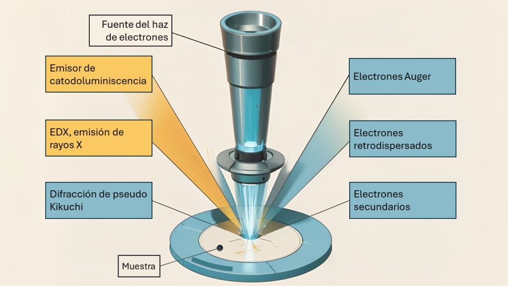
The SEM works by firing a beam of electrons from an electron gun at the sample. This beam is focused and directed by electromagnetic and electrostatic lenses. When the electrons hit the surface of the sample, they generate secondary and backscattered electrons, as well as characteristic X-rays. Each of these signals provides different information: secondary electrons provide detailed images of the surface, while backscattered electrons can reveal information about the contrast of materials. The characteristic X-rays, meanwhile, allow elemental chemical analysis to be carried out by energy dispersive spectroscopy (EDS).
Its unique characteristics include the ability to generate three-dimensional images, which offer a more complete view of surface structure, and the possibility of performing precise chemical analyses at the microscopic level. In addition, scanning electron microscope (SEM) is capable of analysing extremely small areas, with an analysis point size in the nanometre range, making it an indispensable tool for nanoscience and nanotechnology.

How does scanning electron microscope (SEM) work?
The results obtained with the scanning electron microscope (SEM) are interpreted through a detailed analysis of the images and data generated. The following is a description of how some of the most common results are interpreted:
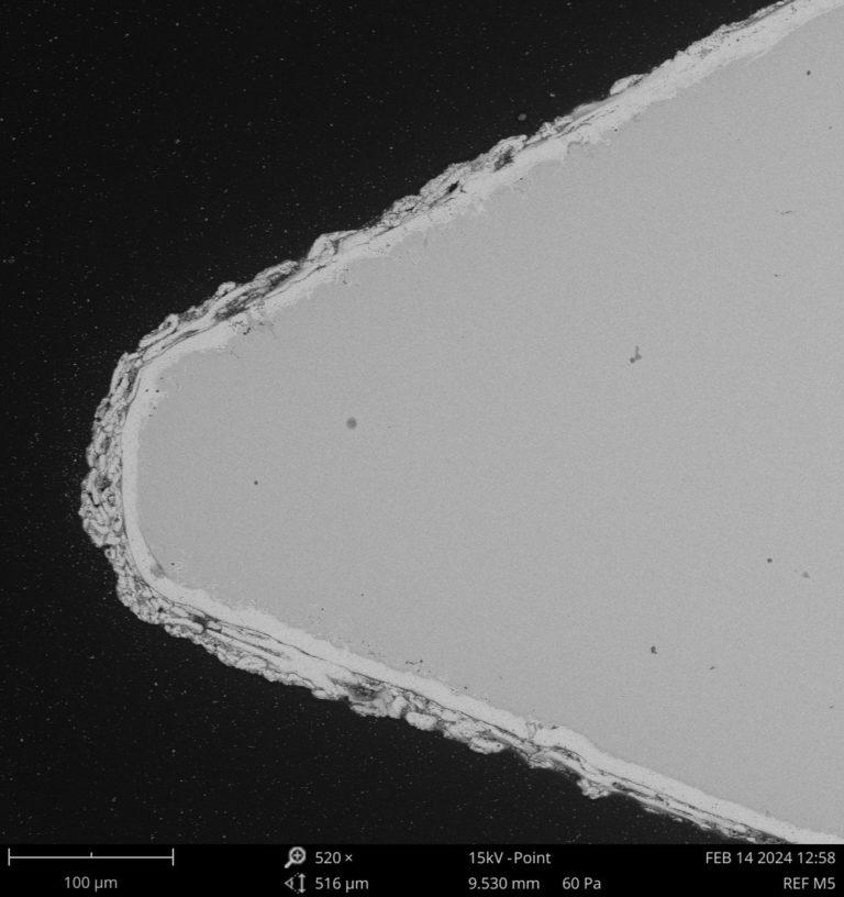
- High Resolution Images: The images produced by the scanning electron microscope (SEM) show the topography and morphology of the surface of the samples on a microscopic scale. The interpretation of these images allows the identification of characteristics such as cracks, defects, and the granular structure of the materials.
- Mapping of Elements: The scanning electron microscope (SEM) can perform chemical analyses using energy dispersive spectroscopy (EDS). This provides a map of the distribution of the elements present in the sample. The interpretation of these maps helps to understand the chemical composition and detect the presence of contaminants or unwanted inclusions.
- Fractographic analysis: By observing fractured surfaces, the failure mode of the material can be determined, whether by brittle, ductile or fatigue fracture. This analysis is crucial for improving the design of materials and manufacturing processes.
- Phase analysis: The identification of different phases in metallic materials is carried out by analysing the diffraction patterns and the morphology of the phases. This allows the mechanical and physical properties of the materials to be optimised.
- Corrosion assessment: By analysing corroded areas, the type of corrosion (uniform, localised, intergranular) and its severity can be determined. This is essential for developing mitigation strategies and selecting more corrosion-resistant materials.

Benefits of using the scanning electron microscope (SEM)
A key benefit of scanning electron microscope (SEM) is its ability to perform detailed analyses without requiring extensive sample preparation. This attribute is especially valuable in contexts where sample preservation is critical, such as in research into biological and archaeological materials and in heritage conservation. Minimal sample preparation not only saves time, but also reduces the risk of introducing artefacts or altering the inherent properties of the material, allowing for more accurate and relevant observations.
Furthermore, the scanning electron microscope (SEM) is highly versatile and can be adapted to diverse analytical needs thanks to its variety of operating modes and complementary techniques. For example, low vacuum modes allow the analysis of non-conductive samples without the need for a metallic coating, while high resolution modes can provide detailed images of nanoscale structures. The integration of complementary techniques, such as energy dispersive spectroscopy (EDS) and electron backscatter diffraction (EBSD), further expands the capabilities of the scanning electron microscope (SEM), allowing not only morphological characterisation, but also chemical identification and determination of crystallographic orientations.
These aspects make the scanning electron microscope (SEM) an indispensable tool in research laboratories, quality control, cases of forensic engineering, as well as in industrial applications where precision and efficiency are fundamental. Its ability to deliver fast and reliable results makes it a preferred choice for a wide range of studies, from materials science to biology, medicine and engineering.
Scanning electron microscope (SEM) equipment
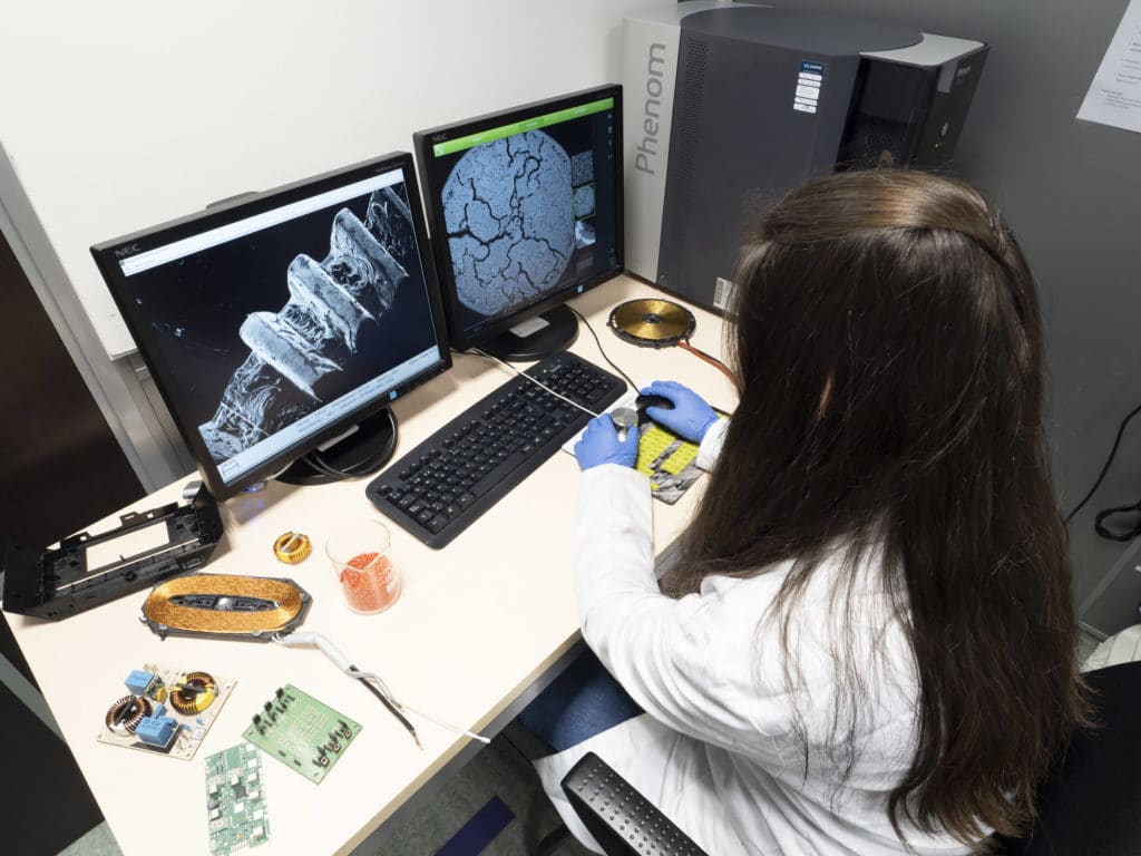
At INFINITIA we have the scanning electron microscope (SEM) Phenom ProX Desktop, a leading model in this category of microscopes. This desktop device combines ease of use with exceptional performance, making it an ideal choice for both academic laboratories and industrial environments. Its compact design and intuitive interface allow users to obtain high-quality results efficiently and accurately.

Applications of scanning electron microscope (SEM)
The scanning electron microscope (SEM) has a wide range of applications in different fields of research and industrial sectors. The most relevant applications include:
Fractographic analysis: it
allows the study of the characteristics of fractures in materials, helping to understand the mechanisms of failure and improve manufacturing processes.
Analysis of metallic phases:
Facilitates the identification and characterisation of the different phases present in metal alloys, crucial for the development of new materials and optimisation of properties.
Defect detection: it
helps in the identification of imperfections and defects in materials and components, guaranteeing the quality and reliability of the final products.
Evaluation of corrosion results:
Allows the degree and type of corrosion in materials to be evaluated, fundamental for the selection of materials and the implementation of preventive measures in industry.
Characterisation of welds:
Provides detailed information on the microstructure and composition of welds, ensuring the integrity and quality of welded joints.
These applications highlight the importance of the SEM (scanning electron microscope) in the advancement of science and technology, providing practical and effective solutions to various challenges in research and industrial production. The SEM is an invaluable tool for those seeking to obtain accurate and detailed data, thus optimising their processes and improving the quality of their products.
Here are some examples of SEM at INFINITIA:
If you need to apply this equipment to one of your projects, don’t hesitate to get in touch. We at Infinitia are here to help.


