What was the challenge or problem to solve?
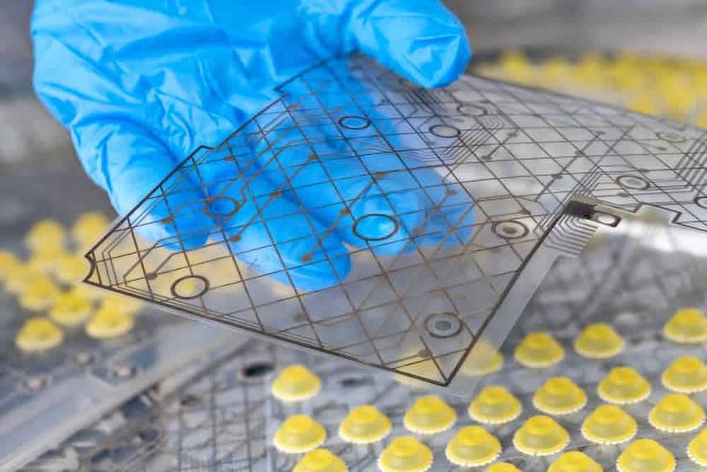
In the field of electronic components manufacturing, one of the most complex challenges is the processing of multilayer materials by laser cutting, especially when precision cutting is required without affecting adjacent layers.
INFINITIA was faced with the need to achieve an accurate cut of certain electronic components. The risk was high: an improper cut could not only damage the material, but also cause short circuits, resulting in the complete unusability of the component.


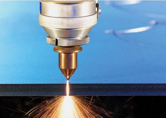
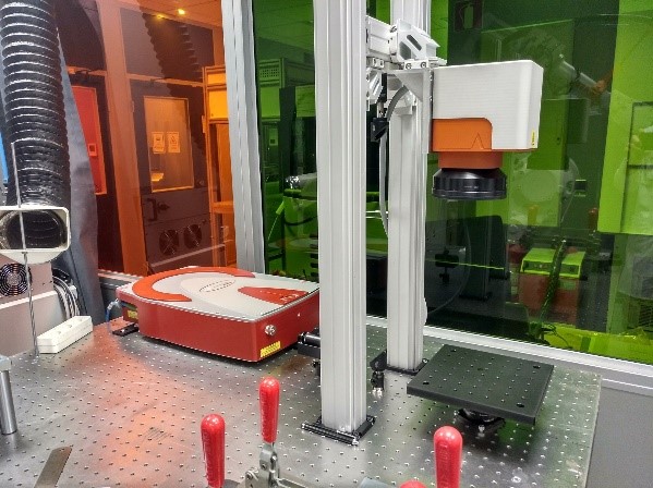
Initially, the use of an ultrashort pulse laser was selected for cutting the multilayer material. This technology was chosen for its ability to emit extremely short pulses, with sufficient repetition rates and spot sizes to provide the precision required for working with delicate materials.
Preparing the sample for proper inspection was the next crucial step. Certain laboratory tools were used, including a diamond saw for cross-cutting the parts and specialized polishing techniques. This process was intended to preserve the integrity of the sample, allowing detailed evaluation of the cuts without significant alterations.
Inspection of the cut surfaces was performed by optical and scanning electron microscopy (SEM), allowing the team to accurately assess the extent and quality of the applied cuts. This stage was fundamental to validate the effectiveness of the selected laser parameters, ensuring that the desired layers were adequately removed without affecting the layers below.

